Basic Electrical Theory

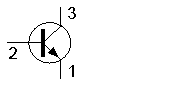
In the figure shown, 2 represents the
-
collector of a pnp transistor
-
emitter of an npn transistor
-
Correct Answerbase of an npn transistor
-
source of a junction FET
Correct answer: C — base of an npn transistor
The symbol shown is a bipolar junction transistor (BJT) of the npn type. In the standard BJT symbol, the arrow on the emitter points outward (away from the base) for an npn transistor, confirming the type. The three terminals are labelled in the diagram as follows:
- 1 — emitter (the terminal with the arrow)
- 2 — base (the horizontal line at the centre-left)
- 3 — collector (the terminal opposite the emitter, no arrow)
Terminal 2 connects to the base, which is the thin central region of the transistor that controls current flow between collector and emitter.
- A is wrong — the symbol is npn, not pnp; in a pnp symbol the arrow points inward toward the base. Terminal 2 is also not the collector in either type.
- B is wrong — terminal 2 is the base lead, not the emitter; the emitter is terminal 1 (identified by the arrow).
- D is wrong — this is a BJT symbol, not a junction FET (JFET); a JFET has a gate, drain, and source, with a different schematic symbol.
Therefore, terminal 2 in this npn BJT symbol represents the base.
Last edited by jim.carroll. Register to edit
In the figure shown, 3 represents the
-
drain of a junction FET
-
Correct Answercollector of an npn transistor
-
emitter of a pnp transistor
-
base of an npn transistor
Correct answer: B — collector of an npn transistor
The symbol shown is a bipolar junction transistor (BJT) of the npn type. The key identifier is the arrow on the emitter lead: in an npn transistor the arrow points outward (away from the base), representing conventional current flowing out of the emitter. The three terminals are:
-
Terminal 1 (bottom) — the emitter (the lead with the outward-pointing arrow)
-
Terminal 2 (left) — the base (the horizontal line connecting to the centre of the device)
-
Terminal 3 (top) — the collector (the lead without an arrow, opposite the emitter)
-
A — drain of a junction FET: Incorrect; a JFET symbol uses a gate line touching a channel bar, not the arrow-on-emitter structure shown here.
-
C — emitter of a pnp transistor: Incorrect; a pnp transistor has its emitter arrow pointing inward (toward the base), and terminal 1, not terminal 3, carries the arrow in any case.
-
D — base of an npn transistor: Incorrect; the base is terminal 2 (the horizontal input lead on the left side of the symbol).
Therefore, terminal 3 in the diagram is the collector of an npn transistor.
Last edited by jim.carroll. Register to edit
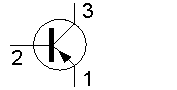
In the figure shown, 2 represents the
-
Correct Answerbase of a pnp transistor
-
drain of a junction FET
-
gate of a junction FET
-
emitter of a pnp transistor
Correct answer: base of a pnp transistor
The symbol shown is a bipolar junction transistor (BJT).
- Terminal 1 is the emitter
- Terminal 2 is the base
- Terminal 3 is the collector
The arrow on the emitter pointing inward indicates a PNP transistor.
- FETs use different symbols (gate, drain, source).
- The emitter is identified by the arrow, not terminal 2.
Therefore, terminal 2 represents the base of a pnp transistor.
Last edited by jim.carroll. Register to edit
In the figure shown, 1 represents the
-
collector of a pnp transistor
-
gate of a junction FET
-
source of a MOSFET
-
Correct Answeremitter of a pnp transistor
Correct answer: emitter of a pnp transistor
The symbol shown is a bipolar junction transistor (BJT). The arrow identifies the emitter, and the direction of the arrow indicates the transistor type:
- an arrow pointing toward the base means a pnp transistor
- an arrow pointing away from the base means an npn transistor
In the diagram, terminal 1 is the lead with the arrow pointing inward toward the base, so it is the emitter of a pnp transistor.
- collector of a pnp transistor is incorrect because the collector does not have an arrow.
- gate of a junction FET is incorrect because this symbol is a BJT, not a FET.
- source of a MOSFET is also incorrect because MOSFET symbols use a different gate and channel structure.
Therefore, terminal 1 represents the emitter of a pnp transistor.
Last edited by jim.carroll. Register to edit
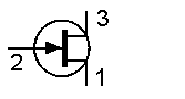
In the figure shown, 2 represents the
-
drain of a p-channel junction FET
-
collector of an npn transistor
-
Correct Answergate of an n-channel junction FET
-
base of a pnp transistor
Correct answer: gate of an n-channel junction FET
The symbol shown is for a junction field-effect transistor (JFET). In this symbol:
- The vertical line represents the channel between the drain and source.
- The terminal with the arrow pointing toward the channel is the gate.
For an n-channel JFET, the arrow on the gate points toward the channel, indicating the direction of conventional current in the p–n junction.
- A drain terminal does not have an arrow in this manner.
- Bipolar transistors use base, collector, and emitter terminals with a different symbol.
- A pnp transistor symbol is distinctly different from a JFET.
Therefore, terminal 2 represents the gate of an n-channel junction FET.
Last edited by jim.carroll. Register to edit
In the figure shown, 3 represents the
-
source of an n-channel junction FET
-
gate of a p-channel junction FET
-
emitter of a pnp transistor
-
Correct Answerdrain of an n-channel junction FET
Correct answer: drain of an n-channel junction FET
The symbol shown is a junction FET (JFET). The arrow on the gate points toward the channel, which identifies it as an n-channel JFET.
In standard JFET symbols:
- the left terminal is the gate
- the top terminal is the drain
- the bottom terminal is the source
Since label 3 is connected to the top terminal, it represents the drain of an n-channel JFET.
- source of an n-channel junction FET is incorrect because the source is the lower terminal in this symbol.
- gate of a p-channel junction FET is incorrect because the arrow direction indicates an n-channel device, and the gate is the left terminal.
- emitter of a pnp transistor is incorrect because this symbol is a FET, not a bipolar transistor.
Therefore, terminal 3 is the drain of an n-channel junction FET.
Last edited by jim.carroll. Register to edit
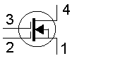
In the figure shown, 2 represents the
-
Correct Answergate of a MOSFET
-
base of a dual bipolar transistor
-
anode of a silicon controlled rectifier
-
cathode of a dual diode
Correct answer: gate of a MOSFET
The symbol shown is for a MOSFET (Metal Oxide Semiconductor Field Effect Transistor).
In this symbol:
-
Terminal 2 is the insulated gate, which controls current flow.
-
Terminals 1 and 4 are the source and drain, forming the conduction path.
-
Terminal 3 is the substrate (body) connection.
-
A bipolar transistor uses base, collector, and emitter terminals.
-
A silicon controlled rectifier has anode, cathode, and gate terminals with a different symbol.
-
A dual diode would show two diode junctions.
Therefore, terminal 2 represents the gate of a MOSFET.
Last edited by jim.carroll. Register to edit
The figure shown represents a
-
dual bipolar transistor
-
dual diode
-
dual varactor diode
-
Correct Answerdual gate MOSFET
Correct answer: dual gate MOSFET
The symbol represents a MOSFET device with two separate gate terminals.
A dual-gate MOSFET has:
- one source
- one drain
- two gates (Gate 1 and Gate 2)
This configuration is commonly used in RF circuits, especially in:
- mixers
- RF amplifiers
because it allows better control of gain and signal mixing.
- A dual bipolar transistor would show two transistor junctions.
- A dual diode would show two diode symbols.
- A varactor diode is a variable capacitance diode, not a transistor.
Therefore, the figure represents a dual gate MOSFET.
Last edited by jim.carroll. Register to edit
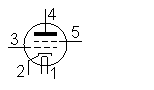
In the figure shown, 3 represents the
-
filament of a tetrode
-
anode of a triode
-
Correct Answergrid of a tetrode
-
screen grid of a pentode
Correct answer: grid of a tetrode
The symbol shown is for a tetrode valve, which has:
- a filament (heater)
- a control grid
- a screen grid
- an anode (plate)
In the diagram, terminal 3 connects to one of the grid structures positioned between the filament and the anode.
- The filament is the heater element at the bottom of the valve.
- The anode is the plate located at the top.
- A pentode would show an additional grid.
Therefore, terminal 3 represents the grid of a tetrode.
Last edited by jim.carroll. Register to edit
In the figure shown, 5 represents the
-
grid of a tetrode
-
Correct Answerscreen grid of a tetrode
-
heater of a pentode
-
grid of a triode
Correct answer: screen grid of a tetrode
The symbol shown is for a tetrode valve, which contains:
- Filament (heater) – heats the cathode
- Cathode – emits electrons when heated
- Control grid – controls electron flow from cathode to anode
- Screen grid – reduces capacitance between control grid and anode
- Anode (plate) – collects electrons to produce current flow
In the diagram:
-
Terminal 1 is the heater (filament)
-
Terminal 2 is the cathode
-
Terminal 3 is the control grid
-
Terminal 4 is the anode
-
Terminal 5 is the screen grid
-
The heater is at the bottom of the symbol.
-
A triode would have only one grid.
Therefore, terminal 5 represents the screen grid of a tetrode.
Last edited by jim.carroll. Register to edit